

Thin Substrate, Dichroic and Polychroic Thin Film Filters Featuring Flatness Less Than Zero Point 1 Waves RMS
Alluxa Introduces a New Line of Ultra-Flat Dichroic and Polychroic High Performance Thin Film Filters that Feature a Flatness of <0.1wave RMS Without the Need for Backside Compensation.
Alluxa is introducing a new line of thin substrate ultra-flat dichroics and polychroic filters for use in imaging applications that require flatness levels exceeding 0.1 waves RMS per inch. These filters are unique because they achieve flatness by eliminating the high stresses of as-deposited traditional ion-based coating process such as Ion Beam Sputtering (IBS) and Ion Assisted Deposition (IAD). Alluxa’s new technique uses a novel plasma coating process that produces low loss, fully dense dielectric films with essentially net zero stress on the primary coated side. This means that the coatings do not require industry standard backside compensation or the use of very thick and expensive substrates to assure flat surface figures. The backside is coated with a simple low cost and high performance Anti-Reflection (AR) coating. Alluxa has achieved flatness levels of <0.1 waves RMS at 632.8 nm per inch with substrates as thin as 0.5mm.
Eliminating backside compensation has a number of important advantages. It lowers total cost by reducing coating thickness. It improves transmission levels by lowering optical scatter and it improves transmitted wave-front properties by lower overall thickness. Eliminating stress in thin film coating also offers the advantage of allowing the thin film engineer much more design freedom to create filters with improved slopes and rejection levels by using more coating layers where previously this may have been impractical.
These new dichroic and polychroic filters are built with fully dense, hard coated refractory oxides using a proprietary high speed plasma deposition technology purpose built for the challenges presented by the latest optical instruments of the life sciences and industrial markets. Reliability has been demonstrated against rigorous Telcordia standards.
Flat Filters: Dichroic and Polychroic Overview
The need for dichroic filters to split one spectral band of light from another has been around for several decades. With the advent of hard coating technologies like high energy sputtering and ion beam sputtering came advances in spectral performance and coating durability. While these processes made and continue to make filters with good spectral performance, the compressive stress levels in the resultant coatings physically distort the finished product by curving the substrate. Because many of these filters work in imaging or laser applications or both, there has been increasing pressure on these filters to meet stringent flatness requirements. In order to achieve the level of flatness or reflected wave-front distortion required in many of these applications, these filters have traditionally been corrected using a technique known as “backside compensation.” In simplistic terms, this compensation technique involves coating both sides of the substrate with a coating that will balance out the stress of the filter and, therefore, flatten the surfaces. The downside of this technique is also straightforward: it can nearly double the amount of coating required and significantly increase the manufacturing cost of the filters.
Following the widespread use of dichroic filters, the need for more complex filters has emerged over the past two decades. Now, applications such as Pinkel and Sedat style fluorescence systems, confocal microscopy, STED, DNA sequencing, and patterned filters have all demonstrated strong demand for flat filters that separate multiple spectral bands from each other at the same time. Bandpass, notch, and multi-band polychroic filters are used to optimize the performance of the instruments. With the added complexity of these filters comes the need for significantly more coating layers than simple dichroic filters. This makes the compensation of these parts even more cumbersome for manufacturing processes utilizing traditional compensation techniques to balance coating stress.
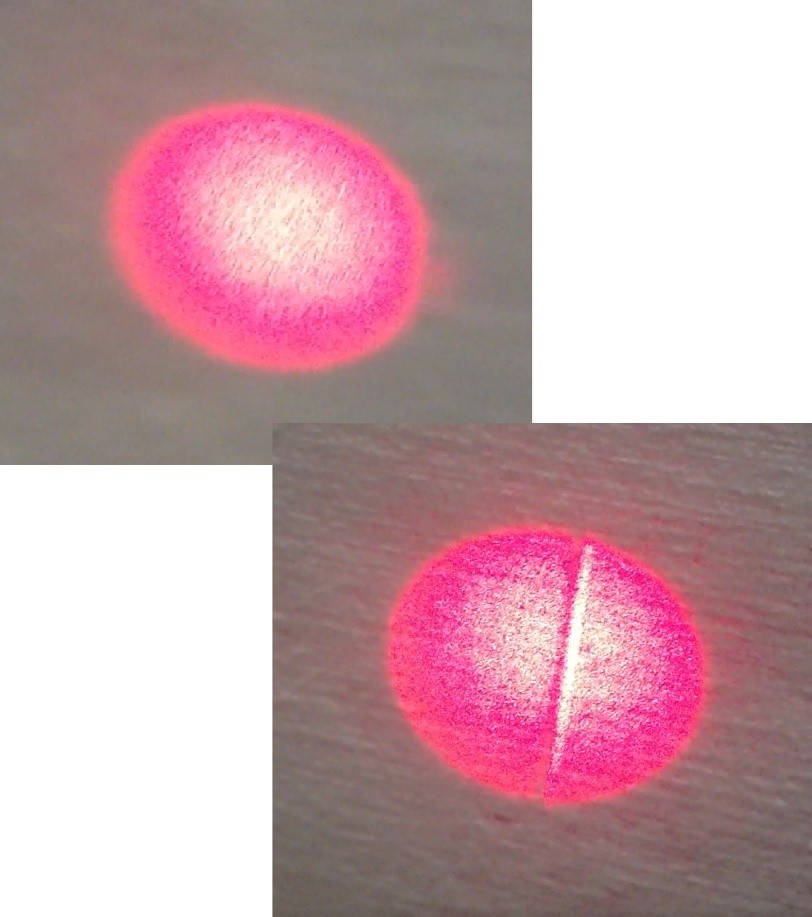
Figure 1 shows representative flatness measurements on a dichroic coated with a standard hard coating process and Figure 2 shows a filter coated using Alluxa’s very low stress coating process. Two examples of very low stress polychroic filters used for confocal microscopy are shown below in Figure 3 and Figure 4.
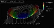
Figure 1. Shows a flatness measurement of a dichroic coated with a standard hard coating process.
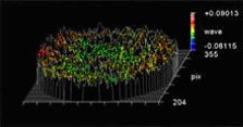
Figure 2. Shows the same dichroic coated using Alluxa’s very low stress process.
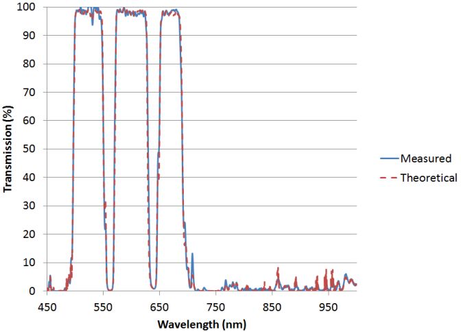
Figure 3. Triple bandpass polychroic on a 1.0 mm thick fused silica substrate with measured flatness of < 0.25 Waves / inch RMS @ 632.8 nm
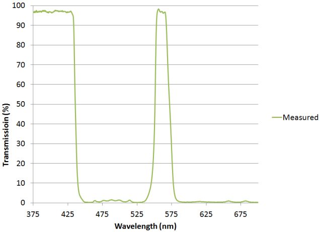
Figure 4. Dual notch polychroic on a 0.5 mm thick fused silica substrate with measured flatness of < 0.25 Waves / inch RMS @ 632.8 nm.
Specifying Dichroic and Polychroic Filters
Specifying dichroics and polychroics filters primarily involves selecting the desired pass bands, blocking bands, substrate type, and thickness. The spectral gaps between the bands is the primary driver of coating complexity and cost.
45 degrees is a standard angle, but the lower the angle the easier it is to achieve performance of slope, blocking and transmission. Similarly, the lower the angular range of the beam, and more collimated, the better the performance in general. Table 1 shows a summary of recommended specifications for polychroic and dichroic filters.
Table 1.
Summary of specifications for Dichroics and Polychroics
| Term/Parameter | Description | High Performance | Standard | Lowest Cost |
| Center wavelength | Center of pass band. This should be used only as a nominal value | +/- 1% (nominal) | +/- 2% (nominal) | +/- 3% (nominal) |
| Pass band Transmission | Transmission average across pass band | >95% | >90% | >85% |
| Pass band width | Range of wavelengths required to transmit | >1% wide 310 – 1100nm | >2% wide 310 nm – 1100nm | >4% wide 310 – 1100nm |
| Blocking band | Range of wavelengths required to suppress | >1% wide 310 – 1100nm | 300 nm – 1100 nm | Optimized for detector and light source |
| Passband to blocking band delta | Spectral gap between the passband and blocking band giving tolerance for slope, centering, etc. | <1% of wavelength | >2% wide 310 nm – 1100nm | Optimized for detector and light source |
| Blocking levels | Blocking suppression levels in log units average over the band | 1% average across blocking band | 5% average across blocking band | 10% average across blocking band |
| Pass band to blocking band gaps | Spectral gap between the pass band and blocking band giving tolerance for slope, centering, etc. | <1% of wavelength | 1% to 3% of wavelength | >3% of wavelength |
| Substrate | Thickness and type | 1mm or less on fused silica | 2mm on fused silica or polished borofloat | Borofloat |
| Flatness | RMS flatness measured at 632nm using interferometer | <0.1wave RMS/inch | 0.5 wave RMS/inch | 1 wave RMS/inch |
Summary
The filters used by fluorescence detection systems are arguably the most important element defining the system performance. Alluxa’s new line of thin substrate ultra-flat dichroics and polychroic filters provide improved optical performance, achieve near zero net stress on the primary coated side, and require only a simple AR coating on the back. Eliminating backside compensation lowers costs, improves transmission levels, reduces scatter and improves transmitted wave-front. Flatness levels of < 0.1 waves RMS at 632 for a one inch part are achievable at thicknesses ranging from 0.5mm and above.
These new polychroic filters are built with fully dense, hard coated refractory oxides using a proprietary high speed plasma deposition technology purpose built for the challenges presented by the latest optical instruments of the life sciences industry.
